Cross-Category Compute, Memory, and Programming Models
4.3.1Compute Engines: Cross-Category Organization and Trade-offs#
Across all four categories, the choice of compute engine — SIMT processors, programmable SIMD units, dedicated matrix engines, vector and scalar units — comes down to two questions.
The first is how much programmability to trade for efficiency. General-purpose execution units and flexible schedulers adapt to more workloads; specialized engines deliver more performance per square millimetre. The second is what computational intensity the target kernels have — how much arithmetic is performed per byte moved across each level of the memory hierarchy. That ratio determines the right balance between compute throughput and memory bandwidth, and it differs between training and inference, which is why the same vendor often ships different engine mixes for each.
GPUs arrived at their present form by accretion. Built originally for graphics, they became highly parallel multithreaded processors with large compute and bandwidth budgets, which is what made general-purpose GPU computing and then deep learning practical on them [1]. Early architectures were dominated by SIMT processors; modern ones add dedicated matrix engines such as NVIDIA's Tensor Cores, reached through specialized PTX instructions and supported by libraries like cuDNN and cuBLAS and by templated abstractions such as CUTLASS and CuTe. Specialized functional units handle transcendentals: the B300 doubles exponential throughput over the B200, reflecting how heavily attention uses those functions [2].
Some architectures carry no matrix engine at all, relying on SIMD or vector units and very high memory bandwidth instead. Cerebras sustains near-peak performance even on the memory-bound BLAS-1 and BLAS-2 levels that fall far short of peak on HBM-based systems [3], and the processing-in-memory designs from Samsung and SK hynix reach high effective bandwidth by placing compute next to DRAM banks [4, 5].
4.3.2Memory Hierarchy: From Hardware Cache to Software Scratchpad#
On-chip SRAM sits on a spectrum from implicit, hardware-managed caches to explicit, software-managed scratchpads. The trade is programmability and compiler simplicity against performance predictability and quality of service.
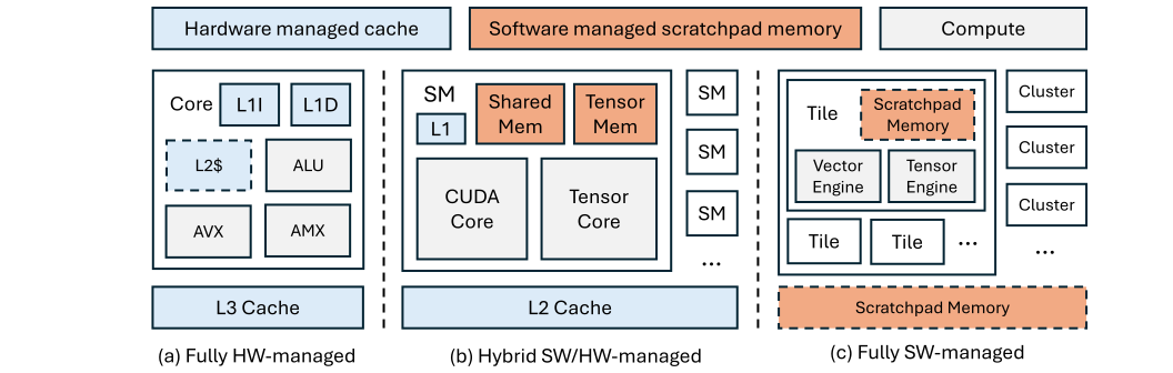
CPUs anchor the hardware-managed end, using multi-level caches where hardware decides placement, replacement and coherence and software addresses a flat space. Generality is excellent, especially for irregular access, but performance analysis is hard because hits, misses and contention all depend on dynamic behaviour. This approach has not left the datacenter: Intel's Gaudi 3 uses configurable SRAM that can serve as a shared L3 or as per-core L2 caches, and adds semantics-aware caching — a Memory Context ID tags lines by algorithmic usage, and allocation hints let developers direct data to L2, L3 or both.
GPUs and domain-specific accelerators expose part of the SRAM instead. NVIDIA partitions each streaming multiprocessor's SRAM between a hardware-managed L1 and software-managed shared memory, so a programmer can orchestrate tiling explicitly while leaving other access patterns to the caches; Blackwell adds a dedicated tensor memory per SM for Tensor Core operands [2]. Scratchpads shift tile sizing, double buffering, prefetch scheduling and synchronization onto the compiler and programmer, and return determinism — the property that makes predictable tail latency, interference isolation and quality-of-service guarantees achievable. AWS NeuronCore is built around this compiler-managed locality model [6].
Memory management is also moving past the chip boundary. NVSHMEM exposes a symmetric memory region on every GPU so kernels can read, write and perform atomics on remote GPU memory over NVLink, PCIe or InfiniBand [7], and Groq backs a logically shared global address space with distributed on-chip SRAM across devices [8].
Compute-in-memory is the complementary extreme, performing simple arithmetic where the data resides rather than staging it into separate arrays — most effective for bandwidth-bound operations with limited reuse, least effective where a matrix engine could have amplified that reuse instead.
References
- 1.Alex Krizhevsky, Ilya Sutskever and Geoffrey E. Hinton. ImageNet Classification with Deep Convolutional Neural Networks. Advances in Neural Information Processing Systems (NeurIPS), 2012.
- 2.Kyle Aubrey and Nick Stam. Inside NVIDIA Blackwell Ultra: The Chip Powering the AI Factory Era. 2025.
- 3.Sean Lie. Cerebras architecture deep dive: First look inside the hardware/software co-design for deep learning. IEEE Micro, 2023.
- 4.Daehan Kwon et al. A 1ynm 1.25 v 8gb 16gb/s/pin gddr6-based accelerator-in-memory supporting 1tflops mac operation and various activation functions for deep learning application. IEEE Journal of Solid-State Circuits, 2023.
- 5.Jin Hyun Kim et al. Aquabolt-XL HBM2-PIM, LPDDR5-PIM with in-memory processing, and AXDIMM with acceleration buffer. IEEE Micro, 2022.
- 6.AWS. NeuronCore-v4 Architecture. 2026. AWS Neuron SDK 2.31.1 documentation.
- 7.NVIDIA. Programming Model Overview. 2020. NVSHMEM 1.0.1 documentation.
- 8.Dennis Abts et al. A software-defined tensor streaming multiprocessor for large-scale machine learning. Proceedings of the 49th Annual International Symposium on Computer Architecture, 2022.