Memory Hierarchy
1.5.2On-Chip SRAM Management: Cache, Scratchpad, and Dedicated Buffers#
On-chip SRAM is the same circuit everywhere; what differs is who decides what lives in it. That choice runs along a spectrum, from caches where the hardware decides implicitly to scratchpads where software decides explicitly. The trade is programmability and compiler simplicity on one end against performance predictability and quality of service on the other.
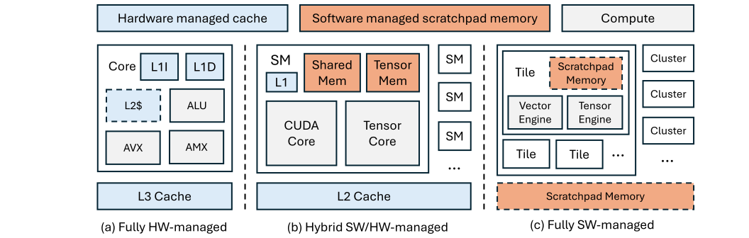
CPUs sit at the hardware-managed end. Multi-level caches decide placement, replacement and coherence on their own, and software gets to pretend it is addressing one flat memory. That is excellent for generality — irregular and data-dependent access patterns are handled without any special effort — but it makes performance hard to reason about, because whether an access hits or misses depends on dynamic execution behaviour you cannot see.
Fully hardware-managed caches have not disappeared from AI accelerators. Intel's Gaudi 3 uses configurable SRAM that can act as one globally shared L3 or as per-core L2 caches, and adds semantics-aware caching on top: a Memory Context ID tags cache lines by how the algorithm uses them, and allocation hints let a developer say whether data belongs in L2, L3, or both.
GPUs and domain-specific accelerators expose part of the SRAM directly. In an NVIDIA GPU the SRAM inside each streaming multiprocessor is partitioned between a hardware-managed L1 cache and a software-managed shared memory. A CUDA programmer allocates shared memory explicitly for tiling, while still letting the L1 and L2 caches handle the accesses that hardware serves better. Blackwell extends this further with a dedicated tensor memory in each SM, reserved for Tensor Core operands [1].
Explicit scratchpads move real work onto the programmer and the compiler: tile sizing, double buffering, prefetch scheduling and synchronization all become part of the performance contract. What you get back is determinism. Data placement and movement are predictable, which is what makes tail latency, interference isolation and quality-of-service guarantees achievable. AWS NeuronCore is built around this compiler-managed locality model [2].
Increasingly, this management extends past the chip. NVSHMEM gives GPUs a distributed shared-memory abstraction: each GPU keeps its own memory, but a symmetric region is exposed on every device so kernels can read, write and perform atomics on remote GPU memory over NVLink, PCIe or InfiniBand [3]. Groq pushes the idea across the network, backing a logically shared global address space with distributed on-chip SRAM. Rather than congestion-aware flow control, it uses software-scheduled networking, where the compiler resolves contention and schedules fine-grained transfers on each link — about 2.5% metadata overhead in exchange for communication behaviour that is highly deterministic [4].
References
- 1.Kyle Aubrey and Nick Stam. Inside NVIDIA Blackwell Ultra: The Chip Powering the AI Factory Era. 2025.
- 2.AWS. NeuronCore-v4 Architecture. 2026. AWS Neuron SDK 2.31.1 documentation.
- 3.NVIDIA. Programming Model Overview. 2020. NVSHMEM 1.0.1 documentation.
- 4.Dennis Abts et al. A software-defined tensor streaming multiprocessor for large-scale machine learning. Proceedings of the 49th Annual International Symposium on Computer Architecture, 2022.